

Why Aluminum Die Cast Housings Need EMI Shielding Engineering
EV power electronics have changed the EMC landscape. Modern traction inverters using SiC MOSFETs switch at 20 kHz–100 kHz with dV/dt exceeding 50 V/ns. The fast edges generate broadband noise from the low kHz range well into the hundreds of MHz. FCC Part 15 Class B sets radiated emission limits; the automotive industry adds CISPR 25, which is significantly tighter — Class 5 limits sit at 18–30 dBµV/m at 1 meter for certain bands.
The aluminum die cast housing is expected to do two jobs simultaneously: thermal management (heat spreading and dissipation) and electromagnetic containment (Faraday cage function). The good news: aluminum alloys are conductive. The bad news: a die cast housing is never a seamless metal box. It has parting lines, ejector pin marks, core prints, machined openings for connectors, and gasket joints — every discontinuity is a slot antenna.
So the real engineering question isn’t "does aluminum shield EMI?" — it does, to a degree. The question is: how do you design and process the die cast housing to close every leakage path and push shielding effectiveness (SE) above the margin your EMC test requires.
Inherent Shielding: What the Die Cast Aluminum Already Gives You
Conductivity of Common Die Cast Alloys
ADC12 (JIS equivalent of A383) and A380 are the workhorses of structural and electronics die casting. Their conductivity is not stellar compared to pure aluminum, but it is sufficient for meaningful shielding.
| Property | ADC12 / A383 | A380 | AlSi10Mg (structural) | Pure Al (reference) |
|---|---|---|---|---|
| Electrical Conductivity (% IACS) | ~23–25 | ~25–27 | ~30–33 | ~62 |
| Thermal Conductivity (W/m·K) | ~96 | ~100 | ~150 | ~237 |
| Density (g/cm³) | 2.74 | 2.71 | 2.68 | 2.70 |
| Tensile Strength (MPa, as-cast) | ~320 | ~320 | ~240 (T6) | low |
At 23–27% IACS, the skin depth at 100 MHz is approximately:
δ = √(2ρ / ωμ) ≈ 13–14 µm for ADC12 at 100 MHz
At 1 GHz, skin depth drops to roughly 4 µm. What this means practically: even a 1 mm wall section provides far more thickness than needed for absorption loss. The wall is not the problem. The joints and openings are.
Shielding Effectiveness: Absorption + Reflection
Total SE (dB) = Reflection Loss (R) + Absorption Loss (A) + Multiple-reflection correction (B)
For a 2 mm ADC12 wall at 100 MHz:
- Reflection loss: ~50 dB (high, because Z_aluminum ≪ Z_free_space)
- Absorption loss: ~40+ dB (wall thickness ≫ skin depth)
- Theoretical SE: well above 90 dB
In practice, we measure 40–60 dB on a well-built housing with properly managed seams. The 30+ dB gap between theory and reality lives entirely in the joints, apertures, and surface-treatment discontinuities. That gap is where this article spends its time.
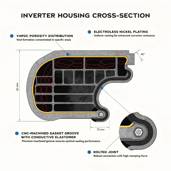
The Porosity Problem: Why VHPDC Is the Foundation of EMI Shielding
Here is where most EMI shielding articles stop telling the truth: porosity in die castings directly degrades shielding and plating quality.
Standard HPDC traps air in the melt. The result is dispersed porosity — micro-voids distributed through the section. Three consequences for EMI:
- Disrupted current path: Porosity breaks up the continuous conductive path. High-frequency currents following the inner skin of the housing encounter voids, increasing transfer impedance at the joint.
- Plating blistering: When you apply electroless nickel or copper plating for enhanced shielding, the plating solution penetrates open porosity. During subsequent thermal cycling, trapped solution outgasses → blisters → shield discontinuity.
- Machined surface porosity: CNC-machined mating faces (where gaskets seat) can expose sub-surface porosity, creating leak paths that conductive gaskets cannot fully bridge.
How VHPDC Addresses This
Vacuum High Pressure Die Casting (VHPDC) evacuates the die cavity before injection. At EMP Tech, all 13 die cast islands from 350T to 3050T are VHPDC-equipped. The measurable outcomes:
| Metric | Standard HPDC | VHPDC (EMP Tech standard) |
|---|---|---|
| Cavity gas content | High (air entrapped) | <5% residual gas |
| Typical porosity (X-ray, volume %) | 3–5% | <1–1.5% |
| Plating blister rate (EN plating) | 5–12% reject | <1% reject |
| X-ray NDT rejection (critical zones) | 2–4% | <0.5% |
This matters because most Tier 1 EMC engineers specify "conductive coating or plating" on die cast housings — and plating quality is entirely gated by substrate integrity. A 5% porosity casting will blister regardless of how good your plating line is.
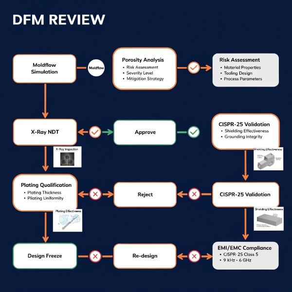
Moldflow-Guided Porosity Management
Even with VHPDC, some residual porosity is industrial reality. We use Moldflow simulation to predict and guide porosity to non-critical zones:
- Porosity is steered toward non-machined, non-mating surfaces
- Machined gasket groove areas are flagged critical — Moldflow optimizes gate and overflow design to keep these zones sound
- X-ray NDT is then targeted at critical zones (gasket seats, plating areas) rather than random sampling
This is what we mean when we say we manage risk through engineering, not by promising zero porosity. Any die caster who claims zero porosity on a 3050T structural part is not being honest with you.
Surface Treatment Options for Shielding Enhancement
Bare aluminum die castings provide 40–60 dB SE depending on joint design. For many EV applications (inverter, motor controller housings), the target is 60–80 dB across the relevant frequency band. That gap is closed by surface treatment plus gasket engineering.
| Treatment | SE Gain (dB, typical) | Conductivity | Corrosion Resistance | Cost Index | Blister Risk |
|---|---|---|---|---|---|
| Bare (as-cast + CNC) | Baseline (40–60) | 23–27% IACS | Poor (oxide forms) | 1.0 | N/A |
| Chromate (Alodine) conversion | 0 to –3 | Reduced (non-conductive) | Good | 1.2 | Low |
| Electroless Nickel (EN) | +10–20 | Moderate | Excellent | 2.5 | Medium (porosity-dependent) |
| Ni/Cu composite plating | +20–35 | High | Good | 3.0 | Medium |
| Zinc flame spray | +15–25 | High | Moderate | 2.0 | Low |
| Conductive silver-pigment paint | +20–40 | High | Moderate | 3.5 | Low |
| Conductive nickel-pigment paint | +10–25 | Moderate | Moderate | 2.0 | Low |
Practical Selection Logic for EV Inverter Housings
For our highest-volume EMI-sensitive product (traction inverter housings), the validated stack is:
- VHPDC substrate (porosity <1.5% in critical zones)
- Targeted CNC surface prep on gasket groove seats (Ra ≤ 1.6 µm, flatness 0.05 mm)
- Electroless nickel on critical inner surfaces (10–15 µm)
- Conductive elastomer gasket in CNC-machined groove (continuous path, no breaks)
- Compression stops to control gasket deflection (15–25% compression)
This stack reliably achieves 65–80 dB SE from 30 MHz to 1 GHz in our CISPR 25 component-level validation runs. It is not the cheapest option, nor the most aggressive — it is the one that passes consistently across production lots without exotic materials or single-source gasket compounds.
Design Features: Gasket Grooves, Seam Continuity, Aperture Control
The Gasket Groove — The Most Critical EMI Feature on the Housing
The conductive elastomer gasket is only as good as its groove. Engineering considerations we enforce in every DFM review:
- Groove width: Sized for 15–25% gasket compression. Over-compression causes cold flow and permanent set; under-compression leaves leak paths.
- Groove land flatness: CNC-machined to 0.05 mm flatness on the gasket land. As-cast surfaces are unacceptable here — casting surface tolerance (±0.2 mm typical) would create uneven compression and localized gaps.
- Compression stops: Molded-in or machined standoffs that prevent over-compression during bolt-up. Without them, the gasket extrudes and loses contact pressure at the center of long spans.
- Corner radius: Gasket grooves must have generous radii at corners. Sharp internal corners cause gasket bunching and gaps — and in die castings, sharp corners are stress concentrractors that promote sink and crack defects.
- Bolt spacing: Maximum bolt pitch is determined by gasket deflection and panel stiffness. For a typical 2 mm die cast wall + 15 mm gasket width: bolt pitch ≤ 40–50 mm.
Aperture and Seam Management
Every opening is a slot antenna. The cutoff frequency for a slot of length L is approximately:
fc = c / (2L)
For a 30 mm gap (longest dimension): fc ≈ 5 GHz. At frequencies below cutoff, SE degradation from a slot is approximately:
SE_slot ≈ 20 log(λ / 2L)
Practical rules we apply in DFM reviews:
- Maximum aperture dimension: keep ≤ λ/20 at the highest frequency of concern
- At 1 GHz: λ/20 = 15 mm — keep all gaps under 15 mm, or use waveguide-beyond-cutoff geometry
- Connector feed-throughs: use EMI-filtered connectors or a continuous conductive gasket around the connector perimeter
- Ventilation openings: use honeycomb waveguide arrays (each cell below cutoff at the frequency of concern)
Bolt and Joint Conductivity
Bolted joints create contact resistance. At high frequencies, RF current flows through the contact interface between mating surfaces, not through the bolts themselves. Contact resistance depends on:
- Surface finish: CNC-machined mating faces at Ra ≤ 1.6 µm
- Contact pressure: target ≥ 1 MPa for continuous low-impedance joint
- Surface treatment: bare aluminum forms oxide within hours — the oxide layer is non-conductive and must be bridged by plating or gasket
This is why we never rely on bare metal-to-metal contact for the EMI path on die castings. The conductive gasket or plating carries the RF current; the bolts provide compression.
Testing and Validation: Shielding Effectiveness
Standards and Methods
| Method | Standard | Frequency Range | What It Measures | Typical Target |
|---|---|---|---|---|
| Shielded enclosure | IEEE Std 299 | 9 kHz – 18 GHz | Global SE of assembled housing | 60–80 dB |
| Transfer impedance | IEC 62153-4 | DC – 1 GHz | Joint and seam quality | <10 mΩ |
| Coaxial transmission line | ASTM D4935 | 30 MHz – 1.5 GHz | Material / plating SE | Treatment comparison |
| Reverberation chamber | IEC 61000-4-21 | 80 MHz – 18 GHz | Realistic emissions | CISPR 25 limits |
| Component-level radiated | CISPR 25 | 150 kHz – 1 GHz | Full-system compliance | Class 4 / 5 |
Our Staged Validation Process
For every new EMI-critical housing program, we run a four-stage validation:
- Material / plating SE: ASTM D4935 coupons cut from same-batch castings, plated alongside production parts. This isolates treatment effectiveness from joint design.
- Joint transfer impedance: IEC 62153-4 on bolted seam samples (plated + gasketed). Pass criterion: <10 mΩ at 1 GHz.
- Assembled housing SE: IEEE 299 in our shielded room — full housing with gasket, hardware, and connectors installed.
- CISPR 25 component-level: The final arbiter. Customer’s electronics installed, running representative duty cycle, emissions measured at 1 m.
A Real DFM Review — Inverter Housing for a German Tier 1
In a recent program, the customer’s EMC team specified "85 dB SE minimum, 30 MHz–1 GHz" on the housing data sheet. First prototype measured 58 dB at 230 MHz — a 27 dB shortfall.
Root cause: the connector cutout ran through a parting line, creating a 45 mm uncontrolled gap that the gasket could not bridge. The fix was not more plating — it was a DFM change: relocating the connector 15 mm off the parting line and adding a CNC-machined gasket land around the full perimeter. Second prototype: 78 dB. The remaining 7 dB to target was closed by upgrading from nickel-graphite to silver-aluminum filled gasket material.
The lesson: roughly 85% of EMI shielding shortfalls on die cast housings are joint and aperture design problems, not material or plating problems. No amount of surface treatment compensates for a 45 mm uncontrolled gap.
Cost and Process Trade-offs
| Approach | Added Cost (% of part cost) | SE Achieved (dB, 30 MHz–1 GHz) | Process Risk | Validation Lead Time |
|---|---|---|---|---|
| Bare + CNC joints, no gasket | 0% | 40–50 | High (oxide, gap variance) | Standard |
| Bare + conductive gasket | +8–12% | 55–65 | Medium (gasket seat tolerance) | +1 week |
| EN plating + gasket | +18–25% | 65–75 | Medium (blister QC) | +2 weeks |
| Ni/Cu plating + silver gasket | +30–40% | 75–85 | Low (well-controlled) | +3–4 weeks |
| Conductive paint (Ag) + gasket | +25–35% | 70–80 | Medium (paint adhesion QC) | +2 weeks |
The pragmatic approach most Tier 1s settle on: EN plating + nickel-graphite gasket — the 80/20 of EMI shielding. It meets CISPR 25 Class 4 for most inverter and motor controller applications, carries manageable process risk, and does not require single-source exotic materials.
We push for VHPDC substrate quality first because it is the cheapest dB you can buy. Improving substrate porosity from 3% to <1.5% can raise plating SE by 5–8 dB and cut plating reject rate by 90% — all for zero added unit cost. That is the first conversation we have in any EMI housing DFM review.
EMP Tech EMI-Relevant Capabilities Summary
| Capability | What It Does for EMI |
|---|---|
| VHPDC (13 islands, 350T–3050T) | Porosity <1.5% → reliable plating substrate → higher SE, lower reject |
| Moldflow porosity management | Guides voids away from gasket seats and plating zones |
| 4/5-axis CNC (150+ machines, single-setup) | Gasket groove flatness 0.05 mm, Ra ≤ 1.6 µm |
| Zeiss CMM | Gasket land dimensional verification to drawing |
| X-ray NDT (targeted) | Inspects critical zones: gasket seats, plating areas |
| In-line helium / air leak testing | Validates joint integrity — gas leak path = EMI leak path |
| IATF 16949:2016 + VDA 6.3 Grade A | Process discipline for repeatable EMI performance lot to lot |
| PPAP Level 3 | Full documentation of shielding-critical characteristics |
Key Takeaways
- Aluminum die cast alloy conductivity is sufficient for shielding — the failures are at joints, apertures, and surface-treatment discontinuities, not in the wall.
- VHPDC is the cheapest SE improvement available. It directly enables better plating and fewer leak paths at zero added unit cost.
- The gasket groove is the most important EMI feature on the housing. Control its flatness, compression, and continuity in DFM — not on the plating line.
- Roughly 85% of shielding shortfalls are joint and aperture design problems, not material or plating problems. Fix them in DFM, not in rework.
- EN plating + nickel-graphite gasket is the pragmatic standard for EV inverter and controller housings — 65–75 dB, manageable risk, no exotic materials.


