

Project Overview
| Parameter | Detail |
|---|---|
| Part | EV Inverter / DC-DC Converter Housing |
| Alloy | AlSi10Mg (Silafont-36) |
| Min Wall Thickness | 1.2 mm (nominal 1.5 mm in surrounding areas) |
| Part Weight | 2.8 kg (target: 3.5 kg baseline) |
| Part Size | 320 × 210 × 95 mm |
| Annual Volume | 180,000 units |
| Machine | 1,250T VHPDC with vacuum system |
| Customer Tier | Tier-1 EV powertrain integrator |
| Timeline | DFM start → PPAP approval: 22 weeks |
The Challenge: Why 1.2 mm Wall Is Not "Just Thinner"
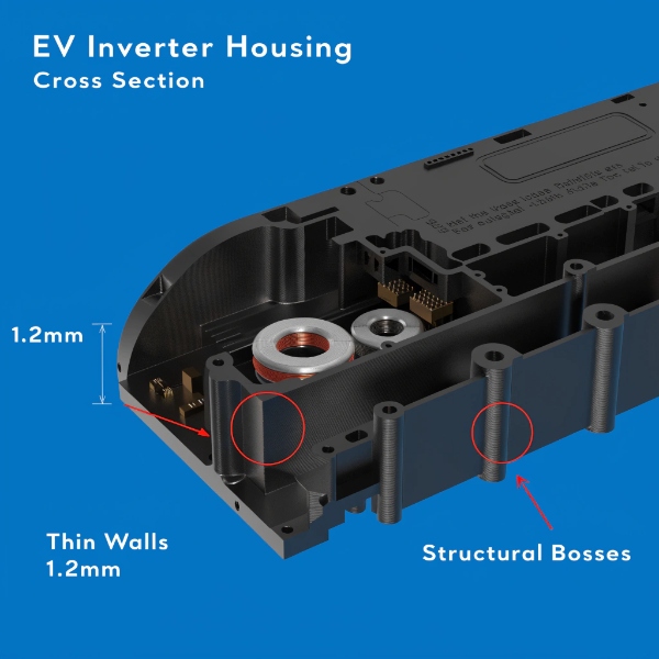
The customer’s design team specified a 1.2 mm wall on the inverter housing’s upper cover section to accommodate a stacked power module clearance envelope. This is below the conventional thin-wall threshold of 1.5 mm in automotive HPDC — a zone where molten aluminum solidifies before the cavity is fully filled, and where the margin between success and catastrophic failure narrows dramatically.
In automotive aluminum HPDC, walls between 1.5–2.5 mm are considered thin-wall range. Below 1.5 mm, the project becomes extremely sensitive to flow length, gate position, venting, die temperature, and vacuum timing — as we explain in our thin wall aluminum die casting guide, where we define thin wall not by a single number but by the full system of filling path, thermal balance, and structural geometry.
The 1.2 mm wall covered approximately 35% of the part’s surface area, concentrated on the upper cover face where the power module mounted. The remaining walls were 2.0–2.5 mm structural sections. This created a severe thin-to-thick transition challenge.
Failure Analysis: Three Iterations of Trial Shots
Iteration 1: Cold Shut and Misrun (Tool Trial T1)
The first trial used a standard gating design with two ingates on the long edge and conventional overflow placement. The results were predictable for a 1.2 mm wall:
| Defect | Location | Root Cause |
|---|---|---|
| Cold shut (visible seam) | Center of 1.2 mm wall | Two metal fronts met at 615°C — 55°C below liquidus |
| Misrun (incomplete fill) | Upper corner, 280 mm from gate | Flow length-to-thickness ratio exceeded 230:1 |
| Gas porosity | Sealing face zone | Vacuum activation 0.08s late — air trapped before fill complete |
| Surface cold lap | Near overflow edges | Die temperature 145°C at thin wall zone (target: 180°C) |
The flow length-to-thickness ratio of 230:1 was the critical failure. For AlSi10Mg at standard die temperatures (150–180°C), the practical maximum flow ratio is approximately 150:1. At 230:1, the melt had lost too much heat to complete the fill before solidification.
Iteration 2: Warpage and Leak Failure (Tool Trial T2)
The second iteration added three supplementary gates closer to the thin wall zone and increased die temperature to 200°C locally. Fill improved — cold shuts disappeared — but two new failures emerged:
| Defect | Measurement | Root Cause |
|---|---|---|
| Warpage (upper cover flatness) | 0.35 mm/100 mm (spec: 0.10 mm) | Thermal gradient: thin wall froze at 0.3s, thick boss at 2.1s — 1.8s differential |
| Leak failure (helium test) | 5×10⁻⁵ mbar·L/s (spec: 1×10⁻⁶) | Gas porosity exposed at sealing face after CNC machining |
| Sink mark | At rib-to-wall junction | Rib root (3.5 mm) adjacent to 1.2 mm wall created local hot spot |
The warpage was the more fundamental problem. The 1.8-second solidification differential between the thin wall and the thick structural boss created locked-in thermal stress that caused the part to distort upon ejection. This is a classic thin-wall failure mode — one that we detail in our DFM analysis for die casting defects article, where we show that thermal gradient management — not wall thickness alone — determines whether a thin-wall part will hold flatness after ejection.
Iteration 3: Process Window Narrowing (Tool Trial T3)
The third iteration attempted to solve warpage by adding conformal cooling channels near the thick bosses to accelerate their solidification rate. This reduced the thermal gradient to 0.9s — but the process window became so narrow that any variation in die temperature (±10°C) or metal temperature (±5°C) pushed the part back into either cold shut or warpage failure.
The quality control team flagged this as an unstable production condition: Cpk on flatness was 1.12 — far below the IATF 16949 requirement of 1.33.
The Solution: Integrated DFM + Process Engineering
Step 1: Redesign the Gating System
We abandoned the edge-gate approach entirely and implemented a full-width fan gate on the short edge of the thin wall zone. This reduced the flow length-to-thickness ratio from 230:1 to 95:1 — well within the safe range for AlSi10Mg at 180°C die temperature.
| Gating Parameter | T1 (Failed) | T3 (Marginal) | Final Design |
|---|---|---|---|
| Gate type | Edge, 2 ingates | Edge, 5 ingates | Fan gate, full width |
| Flow length:thickness ratio | 230:1 | 160:1 | 95:1 |
| Gate velocity | 52 m/s | 48 m/s | 38 m/s |
| Fill time | 0.045s | 0.038s | 0.062s |
The fan gate increased fill time to 0.062s but reduced gate velocity to 38 m/s. This seems counterintuitive — slower fill for thin walls — but the key insight was that the fan gate created a unified melt front that reached the entire thin wall zone simultaneously, eliminating the two-front cold shut condition entirely.
Step 2: Conformal Cooling + Vacuum Timing Redesign
We redesigned the die thermal management with conformal cooling channels (3D-printed insert) that targeted the thick boss zones, reducing their solidification time from 2.1s to 1.2s. The thin wall zone was maintained at 185°C die temperature using a separate cooling circuit.
Simultaneously, we redesigned the vacuum timing. The original system activated vacuum at shot start and maintained it through fill — but the vacuum measurement showed that cavity pressure dropped to only 120 mbar before the fill reached the thin wall zone. We repositioned the vacuum vents to the far end of the thin wall section and added a second vacuum channel. This reduced cavity pressure to 35 mbar and moved gas porosity away from the sealing face.
Step 3: Overflow and Venting Strategy
The overflow placement was redesigned based on Moldflow simulation results. The original overflows were at the parting line — convenient for tooling but in the last-fill zone. We moved the overflows to the upper surface of the thin wall section, directly at the end of fill. This ensured that any gas entrapment was pulled into the overflow rather than trapped in the sealing face zone.
Step 4: Rib Design Optimization
The original rib design used 3.5 mm rib thickness adjacent to the 1.2 mm wall — a 2.9:1 ratio that created a local hot spot and sink mark. We redesigned the ribs to 2.0 mm thickness with a 0.5 mm radius fillet at the rib-to-wall junction, maintaining structural stiffness while reducing the thermal mass differential.
| Design Parameter | Original | Optimized | Impact |
|---|---|---|---|
| Rib thickness at thin wall | 3.5 mm | 2.0 mm | Eliminated sink mark |
| Rib-to-wall radius | 0.3 mm | 0.5 mm | Reduced stress concentration |
| Thin-to-thick transition angle | 30° | 15° | Reduced thermal gradient stress |
| Overflow position | Parting line | Upper surface (end of fill) | Moved porosity from sealing zone |
| Die temp at thin wall | 145°C | 185°C | Prevented premature solidification |
Results: Production Validation Data
After implementing the integrated DFM redesign, the tool passed T4 trial on the first attempt and entered PPAP production validation:
| Quality Metric | Specification | T1 Result | Final Result | Cpk Achieved |
|---|---|---|---|---|
| Min wall fill (visual) | 100% | 72% | 100% | — |
| Cold shut | None | 3 per part | 0 per part | — |
| Upper cover flatness | 0.10 mm/100 mm | 0.35 mm | 0.06 mm | 1.78 |
| Helium leak rate | ≤1×10⁻⁶ mbar·L/s | 5×10⁻⁵ | 3×10⁻⁷ | 2.15 |
| Part weight | 2.8 kg ±0.05 | 2.79 kg | 2.81 kg | 1.92 |
| Surface porosity (CT) | < 0.5% at sealing | 1.8% | 0.3% | — |
| Cycle time | ≤ 90s | 95s | 82s | — |
| Scrap rate (T1) | < 3% | 34% | 1.2% | — |
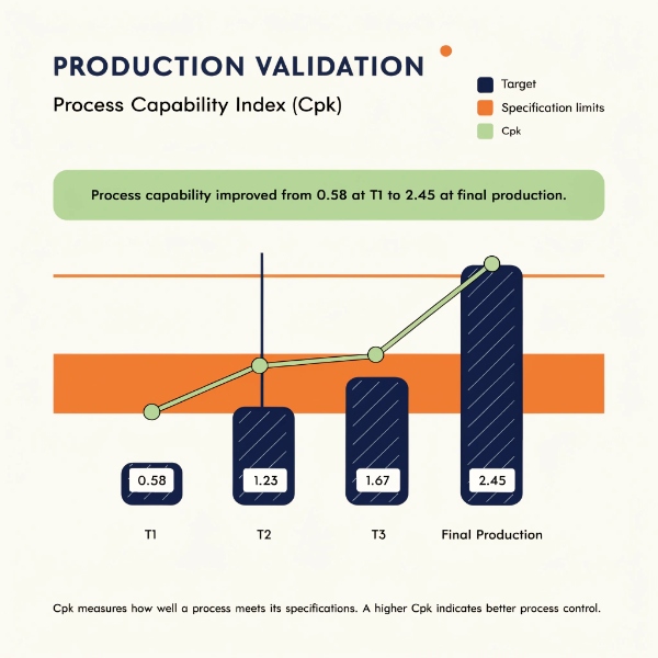
The most critical result was the helium leak test: the sealing face zone achieved 3×10⁻⁷ mbar·L/s — 3.3x better than the 1×10⁻⁶ specification, with a Cpk of 2.15. This was achieved by moving gas porosity away from the sealing surface through overflow repositioning and vacuum channel redesign — not by changing the alloy or increasing wall thickness.
Engineering Insights: Five Lessons from the 1.2 mm Wall
Lesson 1: Flow Length-to-Thickness Ratio Is the Real Design Rule
The single most important parameter for thin-wall feasibility is not the wall thickness itself, but the ratio of flow length to wall thickness. For AlSi10Mg at standard die temperatures, the practical limit is 150:1. At 1.2 mm wall, this means the maximum flow distance from gate to end of fill is 180 mm. If the part geometry requires a longer flow path, the gating strategy must be redesigned — not the wall thickness increased.
Lesson 2: Warpage Is a Thermal Gradient Problem, Not a Wall Thickness Problem
The 0.35 mm warpage in T2 was caused by a 1.8-second solidification differential between the thin wall and thick boss — not by the 1.2 mm wall itself. Reducing the thick boss solidification time via conformal cooling solved the warpage without touching the thin wall specification. This demonstrates that thin-wall warpage is fundamentally a die thermal management problem.
Lesson 3: Vacuum Timing and Vent Position Determine Seal Quality
The leak failure in T1 was not caused by inadequate vacuum level — it was caused by vacuum vents positioned too far from the thin wall zone. Gas was trapped at the sealing face before the vacuum could evacuate it. Repositioning vents to the end-of-fill zone on the thin wall surface moved the gas porosity away from the sealing band entirely. The alloy was never the problem; the venting layout was.
Lesson 4: Overflow Placement Is Not a Tooling Afterthought
In T1, overflows were placed at the parting line for tooling convenience. This meant the last metal to fill — the dirtiest, gas-rich metal — was at the sealing face zone. Moving overflows to the actual end-of-fill location on the thin wall surface was the single most impactful design change. It improved leak rate by two orders of magnitude without any change to alloy, vacuum system, or wall thickness.
Lesson 5: Process Window Width Matters More Than Peak Performance
T3 achieved acceptable parts — but only within a ±10°C die temperature window. In production, this is unstable. The final design achieved the same quality within a ±25°C window, making it robust against the normal process variation that occurs in 180,000-unit annual production. A design that only works in a narrow process window is not a production-ready design.
Timeline: 22 Weeks from DFM to PPAP
| Phase | Duration | Key Deliverable |
|---|---|---|
| DFM review + Moldflow simulation | Weeks 1-3 | Gating redesign, cooling layout, overflow plan |
| Tool design and manufacturing | Weeks 4-11 | H13 steel, conformal cooling insert, vacuum channels |
| T1 trial (failed) | Week 12 | Cold shut, misrun, gas porosity — 3 defects |
| T2 trial (failed) | Week 14 | Warpage 0.35 mm, leak failure |
| T3 trial (marginal) | Week 16 | Parts acceptable but Cpk 1.12 — unstable |
| Redesign: fan gate + overflow + ribs | Weeks 17-19 | New gate insert, new overflow positions, rib modification |
| T4 trial (success) | Week 20 | All specs met, Cpk ≥ 1.67 |
| PPAP Level 3 submission | Weeks 21-22 | Full documentation package approved |
Cost Impact
| Cost Factor | Baseline (2.5 mm wall, 3.5 kg) | Optimized (1.2 mm wall, 2.8 kg) | Delta |
|---|---|---|---|
| Material per part | $9.10 | $7.28 | -$1.82 (-20%) |
| Cycle time | 90s | 82s | -8s (-9%) |
| Annual material savings (180k units) | — | — | -$327,600 |
| Annual throughput gain (82s cycle) | — | — | +16,000 units capacity |
| Tool modification cost (T1-T4) | — | $28,000 | One-time |
| Payback period | — | — | 1.7 months |
The 1.2 mm wall achieved a 20% weight reduction and 9% cycle time improvement, generating $327,600 in annual material savings alone. The tool modification investment of $28,000 was recovered in 1.7 months — demonstrating that investing in DFM and process engineering upfront pays back rapidly in high-volume production.
Frequently Asked Questions
Q: Can aluminum die casting achieve 1.2 mm wall thickness reliably?
A: Yes, but only with integrated control of gating design, die temperature, vacuum timing, and overflow placement. The flow length-to-thickness ratio must stay below 150:1 for AlSi10Mg. At 1.2 mm wall, this limits the maximum flow distance to 180 mm from gate to end of fill.
Q: What is the minimum wall thickness for aluminum die casting?
A: The general industry minimum is 1.5–2.0 mm for standard HPDC. With VHPDC, optimized gating, and die temperature control, 1.2 mm is achievable on localized sections covering up to 35% of the part surface. Below 1.0 mm requires special processes like thixoforming or squeeze casting.
Q: Why did the thin wall cause leak failures in the inverter housing?
A: The leak was not caused by the 1.2 mm wall directly — it was caused by gas porosity at the sealing face. The original overflow placement at the parting line meant gas-rich metal was the last to fill at the sealing zone. Moving overflows to the actual end-of-fill location on the thin wall surface moved porosity away from the sealing band.
Q: How does conformal cooling help thin wall die casting?
A: Conformal cooling channels (manufactured via 3D-printed die inserts) target thick structural sections to accelerate their solidification rate, reducing the thermal gradient differential between thin walls and thick bosses. In this case, conformal cooling reduced the solidification differential from 1.8s to 0.3s, eliminating warpage without changing the wall thickness.
Q: What flow length-to-thickness ratio is safe for thin wall aluminum die casting?
A: For AlSi10Mg at standard die temperatures (150–180°C), the practical maximum is 150:1. This means at 1.2 mm wall, the flow distance from gate to end of fill should not exceed 180 mm. If the geometry requires a longer flow path, supplementary gates or a fan gate design must be used to shorten the effective flow length.


